
15:54Machine-translated from Azerbaijani by AIRead in Azerbaijani
ASML and 3 chipmakers prepare for 6×12-inch chip masks
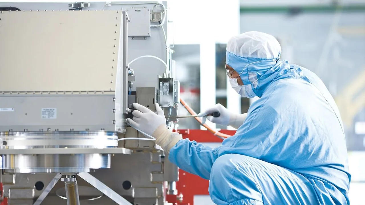
ASML, Intel, Samsung, and TSMC have begun collaborating on a transition to 6×12-inch photomasks for High NA EUV technology. This lithography technology uses light to transfer chip patterns onto a silicon wafer. The photomask serves as the template for that pattern. The new size will make it possible to produce large chips in just 1 exposure step without splitting them into 2 sections. However, the transition will take several years. The current 6×6-inch masks will be used during the initial phase.
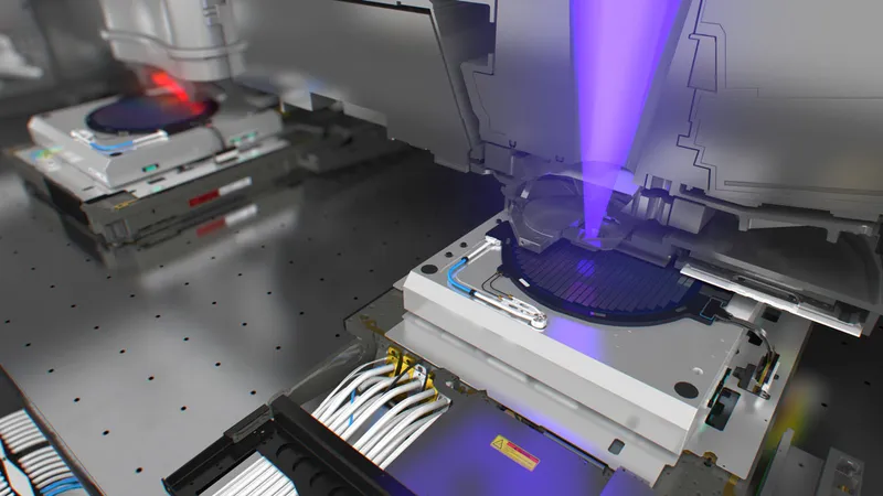
High NA EUV systems have a numerical aperture of 0.55, a measure of their ability to collect light. This equipment achieves a resolution of 8 nm in 1 exposure step. Current EUV scanners with a 0.33 aperture achieve 13 nm. The higher resolution makes it possible to create smaller, more densely packed features in 1 step. This could reduce the number of masks and production steps, accelerate the process, and increase chip yields.
In a High NA EUV system, the current 6×6-inch mask covers an area of only 26×16.5 mm. This field size is sufficient for most consumer processors no larger than 429 mm². For larger central processing units (CPUs) and graphics processing units (GPUs), however, a 26×33 mm pattern must be created in 2 separate exposure steps and stitched together. Another option is to divide the design into smaller chip components, or chiplets. Even a very small alignment error at the stitching boundary can disrupt connections, increase defects, and reduce chip yields.
Stitching together 2 exposure steps also reduces production speed. A scanner that processes up to 175 silicon wafers per hour using a half field processes approximately 125 wafers during stitching. Designers must also account for the stitching boundary and follow additional rules. A 6×12-inch mask restores access to the full 26×33 mm field. This allows a large chip pattern to be created in 1 exposure step.
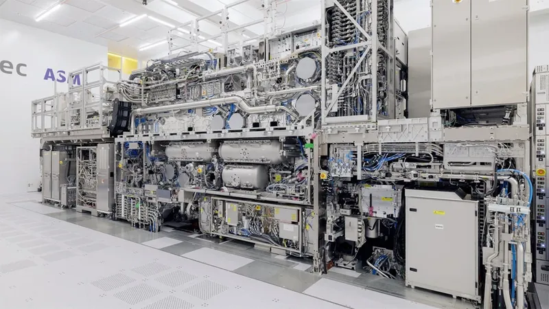
Changing the mask size alone will not be enough to transition to the new format. Manufacturers must upgrade blank mask substrates, pattern-writing and etching equipment, as well as inspection, cleaning, and protective covering systems. ASML scanners must also be modified so that larger masks can be held and moved with high precision. Because the older 6×6-inch format will remain in use, factories must establish storage, transportation, and automated handling systems compatible with both sizes.
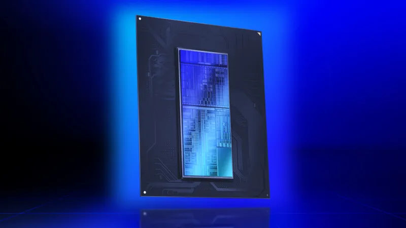
Intel already uses a High NA EUV system for selected Intel 18A layers at its Fab D1X facility. The company supports both half-field and stitching methods. Samsung plans to introduce the technology into mass production of DRAM in 2028. TSMC intends to use it in advanced manufacturing processes starting in 2030. All 3 companies will initially begin with 6×6-inch masks. Although Intel has been working on the larger format for 3 years, it has not announced a transition date.
ASML and TSMC plan to establish a pilot line for the new 6×12-inch photomask in 2031. The goal is for the complete lithography system to be used in advanced chip production to be ready in 2033. Both formats are expected to operate in parallel for a certain period. Large masks will be particularly important for artificial intelligence accelerators, data center CPUs, and high-end GPUs. DPUs, or data processing units, and programmable FPGA chips are also on the list.