
15:28Machine-translated from Azerbaijani by AIRead in Azerbaijani
Intel patents technology for embedding MicroLED lights in chip packaging glass
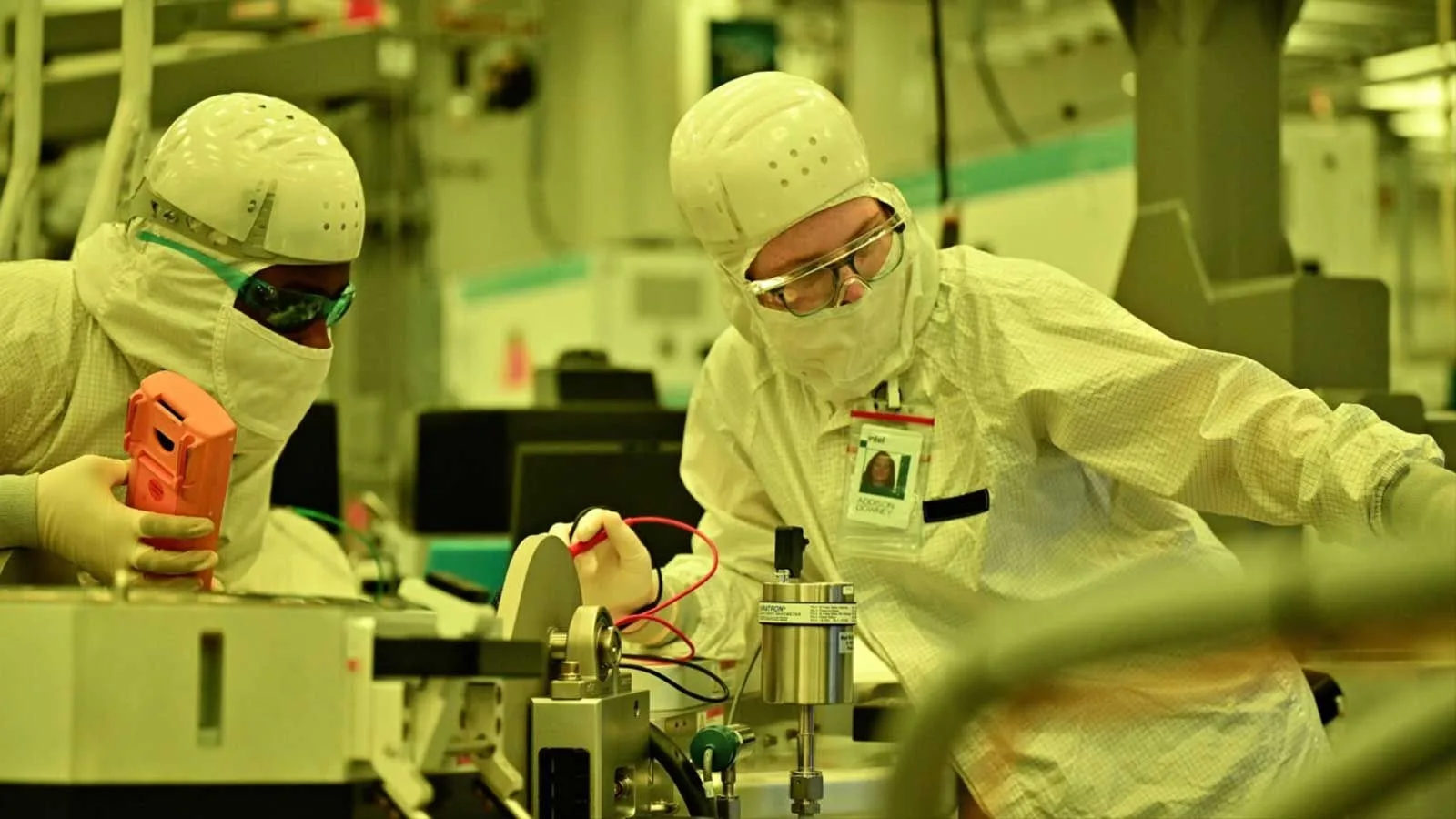
“Intel” has received a U.S. patent covering the placement of MicroLED elements directly into the glass substrate of a chip package. In the design, semiconductor dies containing light sources are embedded in the glass. Electricity and signals are transmitted through conductive channels known as TGVs that pass through the glass. The MicroLED elements can produce red, green and blue light.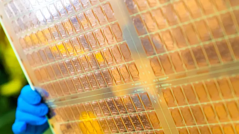 According to the patent, holes and cavities for the dies are created in the glass using lasers and etching. Those channels are then coated with copper, and dies carrying MicroLEDs are placed in the glass substrate. Silicon nitride layers bond the glass to the polymer package sections on both sides. The dies can be positioned both horizontally and vertically. The document also shows reflectors that direct the light in the required direction. “Intel” says this technology could be used to test chips and detect faults. Without the need for a separate indicator, the MicroLED elements in the package could use different light patterns to show that a test has been completed or that a fault has occurred. The patent also covers customizable visual effects such as illuminated text. However, the cooling system could block the light. The solution may therefore be limited to chips that consume less energy or require a special heat sink design.
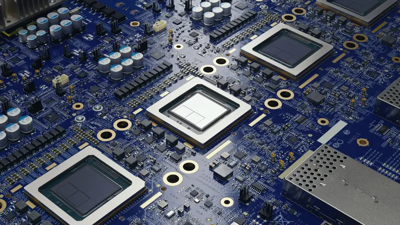 One of the technology’s more important applications is transmitting data within a chip using light signals. “AU Optronics” is developing a module that combines MicroLED transmitters with small light receivers called microphotodetectors and is targeting a connection distance of up to 10 meters. The system, developed for artificial intelligence data centers, was demonstrated at the “SEMICON Taiwan” event in 2026. However, “Intel’s” patent does not describe a complete high-speed optical interconnect system, but rather a chip packaging method compatible with such systems.
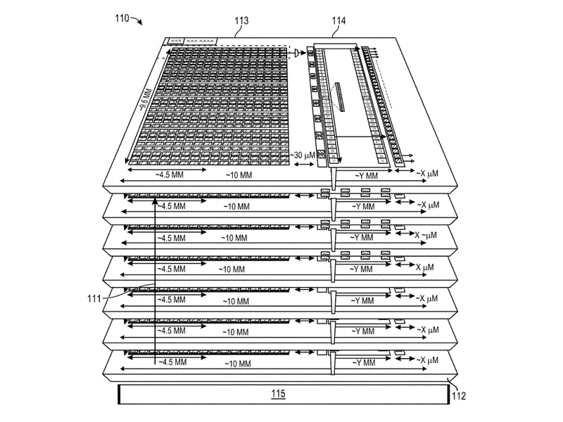 “Intel” has been investing in glass substrate technology since the early 2010s. At the “NEPCON Japan” event in January 2026, the company showed a prototype combining its EMIB multi-chip module technology with a glass-core package. In May, it also demonstrated a 24-layer glass-core panel with copper-filled TGVs and 2 internal EMIB bridges. The results showed progress toward preparing these substrates for mass production. “AU Optronics’” technology roadmap aligns with the approach described in the “Intel” patent. The companies could therefore potentially collaborate in the future. Such a partnership could accelerate the development of a solution combining transmitters, receivers and optical fibers in a single module. For now, however, the patent only describes a method for placing MicroLED elements in a glass package. “Intel” has not announced an official plan for a complete optical interconnect system or its commercial use.
According to the patent, holes and cavities for the dies are created in the glass using lasers and etching. Those channels are then coated with copper, and dies carrying MicroLEDs are placed in the glass substrate. Silicon nitride layers bond the glass to the polymer package sections on both sides. The dies can be positioned both horizontally and vertically. The document also shows reflectors that direct the light in the required direction. “Intel” says this technology could be used to test chips and detect faults. Without the need for a separate indicator, the MicroLED elements in the package could use different light patterns to show that a test has been completed or that a fault has occurred. The patent also covers customizable visual effects such as illuminated text. However, the cooling system could block the light. The solution may therefore be limited to chips that consume less energy or require a special heat sink design. One of the technology’s more important applications is transmitting data within a chip using light signals. “AU Optronics” is developing a module that combines MicroLED transmitters with small light receivers called microphotodetectors and is targeting a connection distance of up to 10 meters. The system, developed for artificial intelligence data centers, was demonstrated at the “SEMICON Taiwan” event in 2026. However, “Intel’s” patent does not describe a complete high-speed optical interconnect system, but rather a chip packaging method compatible with such systems. “Intel” has been investing in glass substrate technology since the early 2010s. At the “NEPCON Japan” event in January 2026, the company showed a prototype combining its EMIB multi-chip module technology with a glass-core package. In May, it also demonstrated a 24-layer glass-core panel with copper-filled TGVs and 2 internal EMIB bridges. The results showed progress toward preparing these substrates for mass production. “AU Optronics’” technology roadmap aligns with the approach described in the “Intel” patent. The companies could therefore potentially collaborate in the future. Such a partnership could accelerate the development of a solution combining transmitters, receivers and optical fibers in a single module. For now, however, the patent only describes a method for placing MicroLED elements in a glass package. “Intel” has not announced an official plan for a complete optical interconnect system or its commercial use.